- 您现在的位置:买卖IC网 > Sheet目录286 > 24AA025E48T-I/SN (Microchip Technology)IC EEPROM SER 2K I2C 8-SOIC
�� �
�
�24AA02E48/24AA025E48�
�5.0� DEVICE� ADDRESSING�
�A� control� byte� is� the� first� byte� received� following� the�
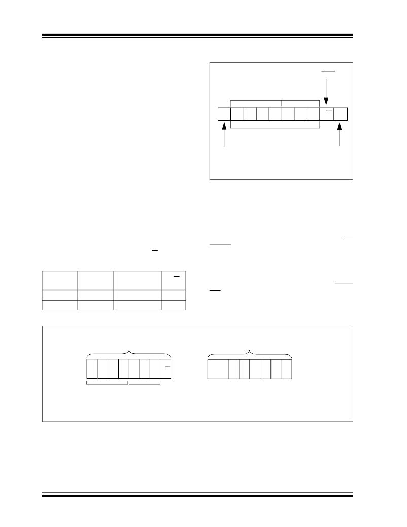
�FIGURE� 5-1:�
�CONTROL� BYTE�
�ALLOCATION�
�Start� condition� from� the� master� device.� The� control� byte�
�consists� of� a� four-bit� control� code.� For� the�
�24AAXXXE48,� this� is� set� as� ‘� 1010� ’� binary� for� read� and�
�write� operations.� For� the� 24AA02E48� the� next� three�
�bits� of� the� control� byte� are� “don’t� cares”.�
�Control� Code�
�Read/Write� Bit�
�Chip�
�Select�
�Bits�
�For� the� 24AA025E48,� the� next� three� bits� of� the� control�
�byte� are� the� Chip� Select� bits� (A2,� A1,� A0).� The� Chip�
�S�
�1�
�0�
�1�
�0�
�A2*� A1*� A0*� R/W� ACK�
�Select� bits� allow� the� use� of� up� to� eight� 24AA025E48�
�devices� on� the� same� bus� and� are� used� to� select� which�
�device� is� accessed.� The� Chip� Select� bits� in� the� control�
�Slave� Address�
�byte� must� correspond� to� the� logic� levels� on� the� corre-�
�sponding� A2,� A1� and� A0� pins� for� the� device� to� respond.�
�These� bits� are� in� effect� the� three� Most� Significant� bits� of�
�the� word� address.�
�For� the� 6-pin� SOT-23� package,� the� A2� address� pin� is�
�Start� Bit�
�Note:�
�Acknowledge� Bit�
�*� Bits� A0,� A1� and� A2� are� “don’t� cares”� for�
�the� 24AA02E48.�
�not� available.� During� device� addressing,� the� A2� Chip�
�Select� bit� should� be� set� to� ‘� 0� ’.�
�The� last� bit� of� the� control� byte� defines� the� operation� to�
�5.1�
�Contiguous� Addressing� Across�
�Multiple� Devices�
�be� performed.� When� set� to� ‘� 1� ’,� a� read� operation� is�
�selected.� When� set� to� ‘� 0� ’,� a� write� operation� is� selected.�
�Following� the� Start� condition,� the� 24AAXXXE48� moni-�
�tors� the� SDA� bus,� checking� the� device� type� identifier�
�being� transmitted� and,� upon� a� ‘� 1010� ’� code,� the� slave�
�device� outputs� an� Acknowledge� signal� on� t� h� e� SDA� line.�
�Depending� on� the� state� of� the� R/W� bit,� the�
�24AAXXXE48� will� select� a� read� or� write� operation.�
�The� Chip� Select� bits� A2,� A1� and� A0� can� be� used� to�
�expand� the� contiguous� address� space� for� up� to� 16K� bits�
�by� adding� up� to� eight� 24AA025E48� devices� on� the�
�same� bus.� In� this� case,� software� can� use� A0� of� the� con-�
�trol byte� as� address� bit� A8,� A1� as� address� bit� A9� and�
�A2� as� address� bit� A10.� It� is� not� possible� to� sequentially�
�read� across� device� boundaries.�
�For� the� SOT-23� package,� up� to� four� 24AA025E48�
�Operation�
�Read�
�Write�
�Control�
�Code�
�1010�
�1010�
�Chip� Select�
�Chip� Address�
�Chip� Address�
�R/W�
�1�
�0�
�devices� can� be� added� for� up� to� 8K� bits� of� address�
�space.� In� this� case,� software� can� us� A0� of� the� control�
�byte� as� address� bit� A8,� and� A1� as� address� bit� A9.� It� is�
�not� possible� to� sequentially� read� across� device�
�boundaries.�
�FIGURE� 5-2:�
�ADDRESS� SEQUENCE� BIT� ASSIGNMENTS�
�Control� Byte�
�Address� Low� Byte�
�1�
�0�
�1�
�0� A2*� A1*� A0*� R/W�
�A�
�7�
�?�
�?�
�?�
�?�
�?�
�?�
�A�
�0�
�Control�
�Code�
�Chip�
�Select�
�bits�
�Note:�
�DS22124D-page� 8�
�*� Bits� A0,� A1� and� A2� are� “don’t� cares”� for� the� 24AA02E48.�
�?� 2010� Microchip� Technology� Inc.�
�发布紧急采购,3分钟左右您将得到回复。
相关PDF资料
24AA02H-I/MS
IC EEPROM 2KBIT 400KHZ 8MSOP
24AA02T/ST
IC EEPROM 2KBIT 400KHZ 8TSSOP
24AA08/ST
IC EEPROM 8KBIT 400KHZ 8TSSOP
24AA16-I/STG
IC EEPROM 16KBIT 400KHZ 8TSSOP
24AA256-I/MS
IC EEPROM 256KBIT 400KHZ 8MSOP
24AA32A/SN
IC EEPROM 32KBIT 400KHZ 8SOIC
24AA32AF-I/SN
IC SRL EEPROM 4KX8 1.8V 8-SOIC
24AA512-I/ST14
IC EEPROM 512KBIT 400KHZ 14TSSOP
相关代理商/技术参数
24AA025E48T-IOT
制造商:MICROCHIP 制造商全称:Microchip Technology 功能描述:2K I2C? Serial EEPROMs with EUI-48? Node Identity
24AA025E48T-ISN
制造商:MICROCHIP 制造商全称:Microchip Technology 功能描述:2K I2C? Serial EEPROMs with EUI-48? Node Identity
24AA025E48-TOT
制造商:MICROCHIP 制造商全称:Microchip Technology 功能描述:2K I2C? Serial EEPROMs with EUI-48? Node Identity
24AA025E48-TSN
制造商:MICROCHIP 制造商全称:Microchip Technology 功能描述:2K I2C? Serial EEPROMs with EUI-48? Node Identity
24AA025E48T-TOT
制造商:MICROCHIP 制造商全称:Microchip Technology 功能描述:2K I2C? Serial EEPROMs with EUI-48? Node Identity
24AA025E48T-TSN
制造商:MICROCHIP 制造商全称:Microchip Technology 功能描述:2K I2C? Serial EEPROMs with EUI-48? Node Identity
24AA025E64
制造商:MICROCHIP 制造商全称:Microchip Technology 功能描述:2K I2Ca?¢ Serial EEPROMs with EUI-48a?¢ or EUI-64a?¢ Node Identity
24AA025E64-E/SN
功能描述:IC EEPROM 2KBIT 制造商:microchip technology 系列:- 包装:管件 零件状态:有效 格式 - 存储器:EEPROM - 串行(带 MAC 地址) 存储器类型:EEPROM 存储容量:2K(256 x 8) 速度:100kHz,400kHz 接口:I2C,2 线串口 电压 - 电源:1.7 V ~ 5.5 V 工作温度:-40°C ~ 125°C(TA) 封装/外壳:8-SOIC(0.154",3.90mm 宽) 供应商器件封装:8-SOIC 标准包装:100